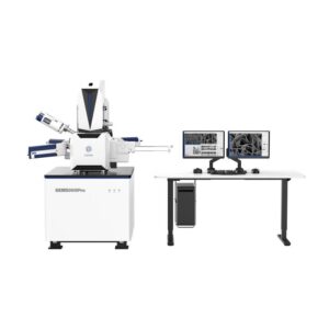
CIQTEK SEM5000Pro Ultra-High Resolution Schottky FESEM
Overview
The SEM5000Pro field-emission scanning electron microscope is designed for stability, reliability, ease of use, and productivity, bringing field-emission imaging capabilities to a wide range of laboratories. Combining ultra-high spatial resolution with long-term operating stability, it consistently delivers high-quality images for applications ranging from advanced nanomaterials characterization to semiconductor R&D and manufacturing, meeting the demanding needs of research institutions and industrial quality-control laboratories.
Application:
– Nano Science
– Semiconductor
– Automobile
– Chemistry
– Electronics
– Pharmaceutical
Benefits & features
– High Resolution
– Multi-detector Technology
– Simplified Alignment
– Built from a Higher-end Platform
– Ultra Beam Deceleration Mode Technology
– Excellent Expandability
Electron Optics
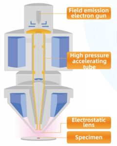
“Super Tunnel” electron optics column technology/in-lens beam deceleration. Decrease spatial charging effect, ensuring low voltage resolution.
Crossover-free in the electron beam path Effectively reduce lens aberrations and improve resolution.
Electromagnetic & electrostatic compound objective lens Reduce aberrations, significantly improve resolution at low voltages, and enable observation of magnetic samples.
Water-cooled constant-temperature objective lens Ensure the stability, reliability, and repeatability of the objective lens operation.
Variable multi-hole aperture with electromagnetic beam deflection system Automatic switching between apertures without mechanical motion, allowing fast switching between imaging modes.
Low-voltage High-resolution Images
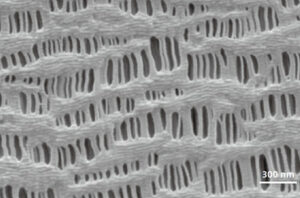
In-lens electron detector image at 200 V low excitation voltage, achieves non-destructive morphological characterization of lithium-ion polymer membrane fiber structures.
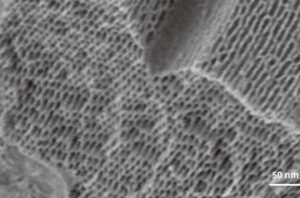
The pore structure of SBA-15 silica-based mesoporous material characterization, In-lens electron detector image at 500 V low voltage without conductive coating (under dual deceleration mode with In-lens beam deceleration + specimen stage tandem beam deceleration).
In-lens Electron Detector / Specimen
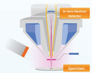
In-lens Electron Detector / Specimen
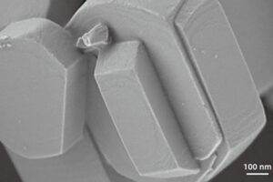
ZSM-8 molecular sieve, a typical catalyst across multiple frontier research fields. Low-voltage imaging without conductive coating provides direct characterization of the surface details of the molecular sieve particles.
Everhart-Thornley Detector (ETD)
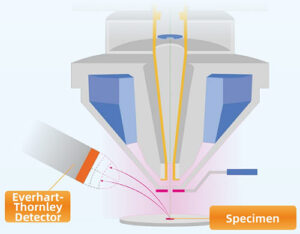
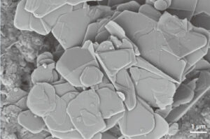
BN ceramic nano-sheets, expose layer structure under low-voltage ETD image
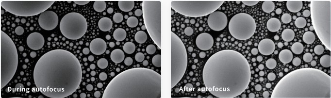
Automatic Brightness & Contrast
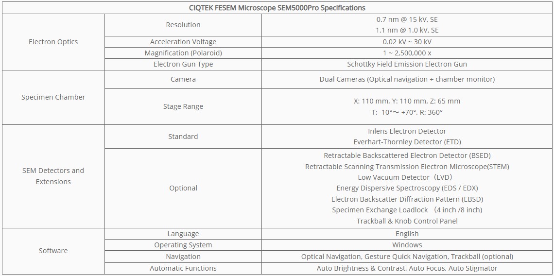
Specifications


 Cell:+65 63821638
  Email: info26@micro-optics.co.id